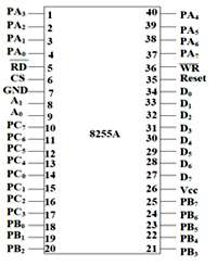
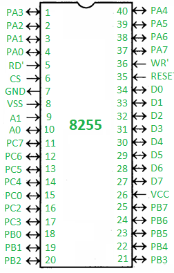
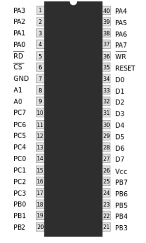
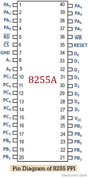
Pin Diagram Of 8255 Ppi
Intel 8255a Pin Description Tutorialspoint
Programmable Peripheral Interface 8255 Geeksforgeeks
Pin Diagram Of 8255 Ppi Programmable Peripheral Interface

Pin Diagram Of 8255 Ppi Open Graduates
8255 Pin Diagram 8255 Block Diagram Modes Of Operation Of 8255

8255 Programmable Peripheral Interface In Depth Simple Explanation
We will study the complete ic structure of it and will also study the functionalities that are performed by each of the pins.
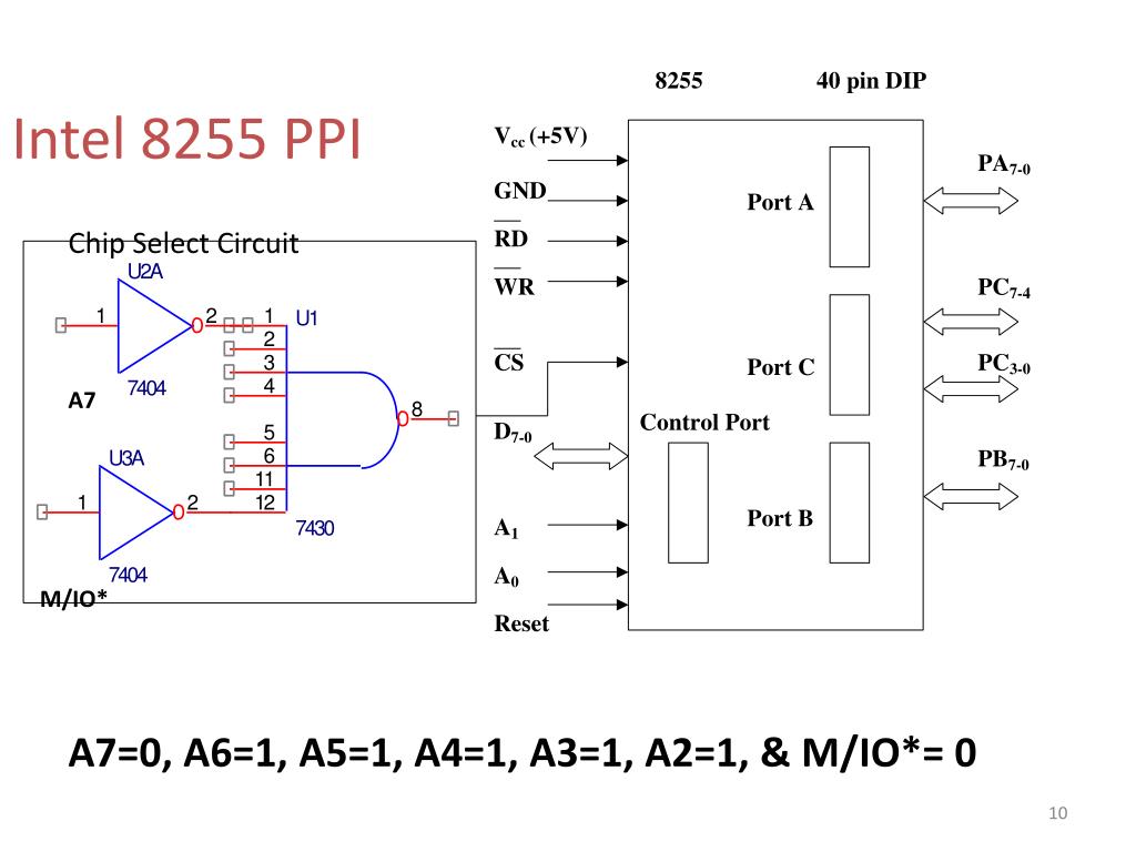
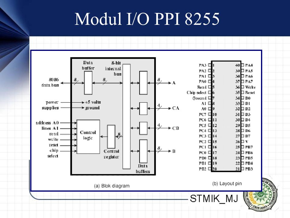
Pin diagram of 8255 ppi. We can program it according to the given condition. Pin diagram of 8255 ppi. Block diagram and pin diagram of 8255. 14 1 shows the 8255 pin diagram of microprocessor.
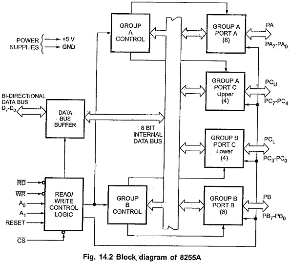
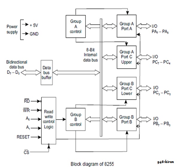
Every one of the ports can be configured as either an input port or an output port. The groups are denoted by port a port b and port c respectively. The intel 8255 or i8255 programmable peripheral interface ppi chip was developed and manufactured by intel in the first half of the 1970s for the intel 8080 microprocessor. 14 2 shows the internal 8255 block diagram of 8255 pin diagram microprocessor.
Here you can see that we have 8 bit of internal bus for the 8255 ppi. In this article we are going to study the pin diagram of the 8255 ppi programmable peripheral interface. Pin diagram pa0 pa7. It consists of data bus buffer control logic and group a and group b controls.
These are tri state data bus lines of bidirectional nature that connects 8255 with the processor. Data is transmitted or received by the buffer as per the instructions by the cpu. Pin diagram of 8255 ppi 8255 pin diagram 11. Submitted by monika sharma on august 16 2019 the following is the internal structure of the 8255 ic.
Function of pins pin function of pin d0 d7 data bus these are bidirectional tri state data bus lines are connected to the system data bus. The 8255 has 24 i o pins divided into 3 groups of 8 pins each. Ppi 8255 is a general purpose programmable i o device designed to interface the cpu with its outside world such as adc dac keyboard etc. Let us first take a look at the pin diagram of intel 8255a now let us discuss the functional description of the pins in 8255a.
They are used to transfer data and control word from microprocessor 8085 to 8255 or receive data or status word from 8255 to the 8085. 8255 pin diagram explanation. The 8255 provides 24 parallel input output lines with a variety of programmable operating modes. This tri state bi directional buffer is used to interface the internal data bus of 8255.
The 8255 is a member of the mcs 85 family of chips designed by intel for use with their 8085 and 8086 microprocessors and. It is a tri state 8 bit buffer which is used to interface the microprocessor to the system data bus. It is further explained as follows. It can be used with almost any microprocessor.

Dac 1408a Chip Hardware Pin Diagram Electrodiction Full Funda Projects To Try Projects
Data Flow Diagram Of 8255 Ppi Programmable Peripheral Interface

8255 Bsr Mode Ppi Hardware Youtube Projects To Try Weather
What Is 8255 Programmable Peripheral Interface Ppi Definition Architecture Pin Diagram And Modes Of Operation Of 8255 Electronics Desk

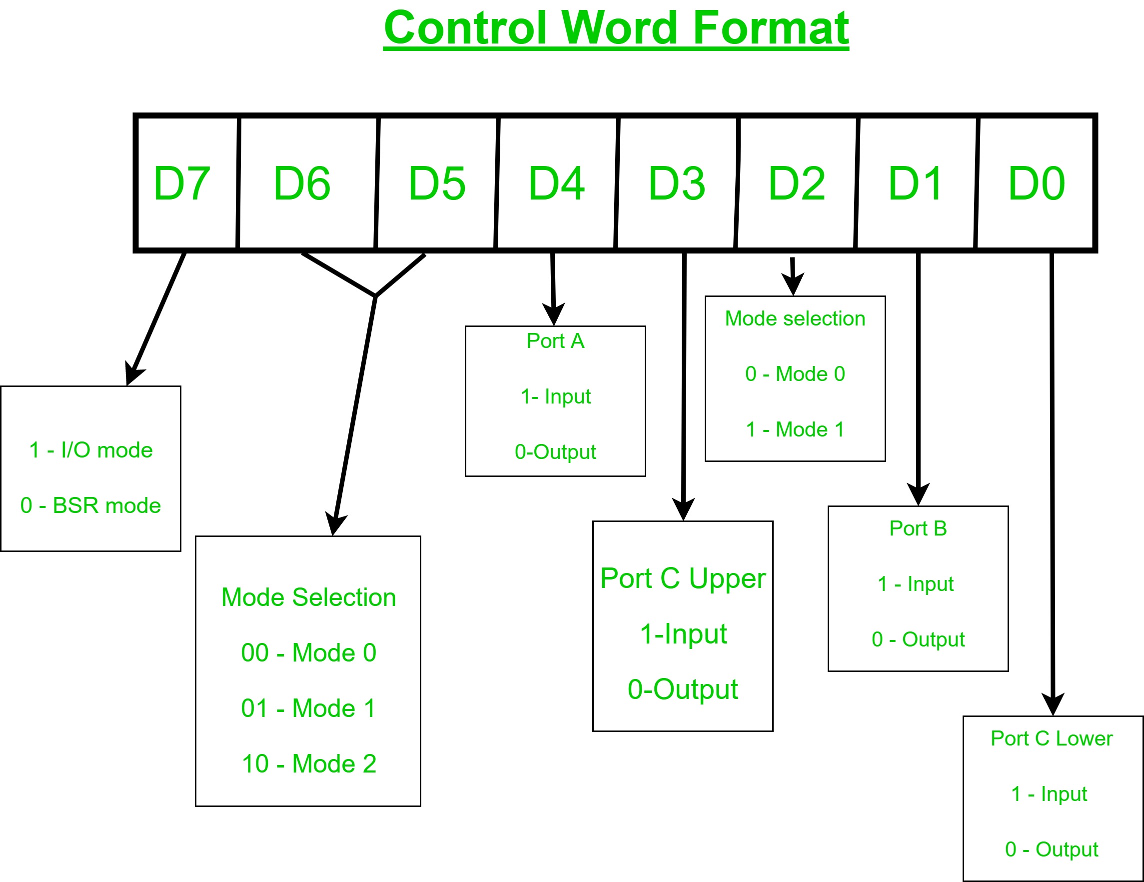
Programmable Peripheral Interface 8255 Architecture Pin Diagram Operational Modes And Control Word Format

Mengambil Input Dari Saklar Di Port B Dan Menampilkan Di Port A Dan Power Strip

The 8255a Programmable Peripheral Interface

Controller Circuit Schematic Peripheral Interface In The Project Of Pressure Monitoring
Microprocessor 8255 Programmable Peripheral Interface Geeksforgeeks
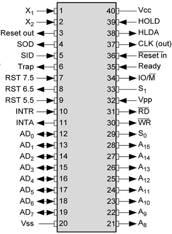
Microprocessor 8085 Pin Configuration Tutorialspoint
Organisasi Komputer Pertemuan 10 Tata Sumitra M Kom Hp Ppt Download
Ppt 8255 Ppi Powerpoint Presentation Free Download Id 5609869

Free Download Biodata Format In Word Sample Template Example Of Excellentcv Resume Curriculum Vitae With Care Curriculum Vitae Biodata Format Curriculum
